This research was done using
Done using
Lightning
Enabling the Acquisition of Electron Beam-Induced Current (EBIC) Images in Conventional SEM and STEM Instruments
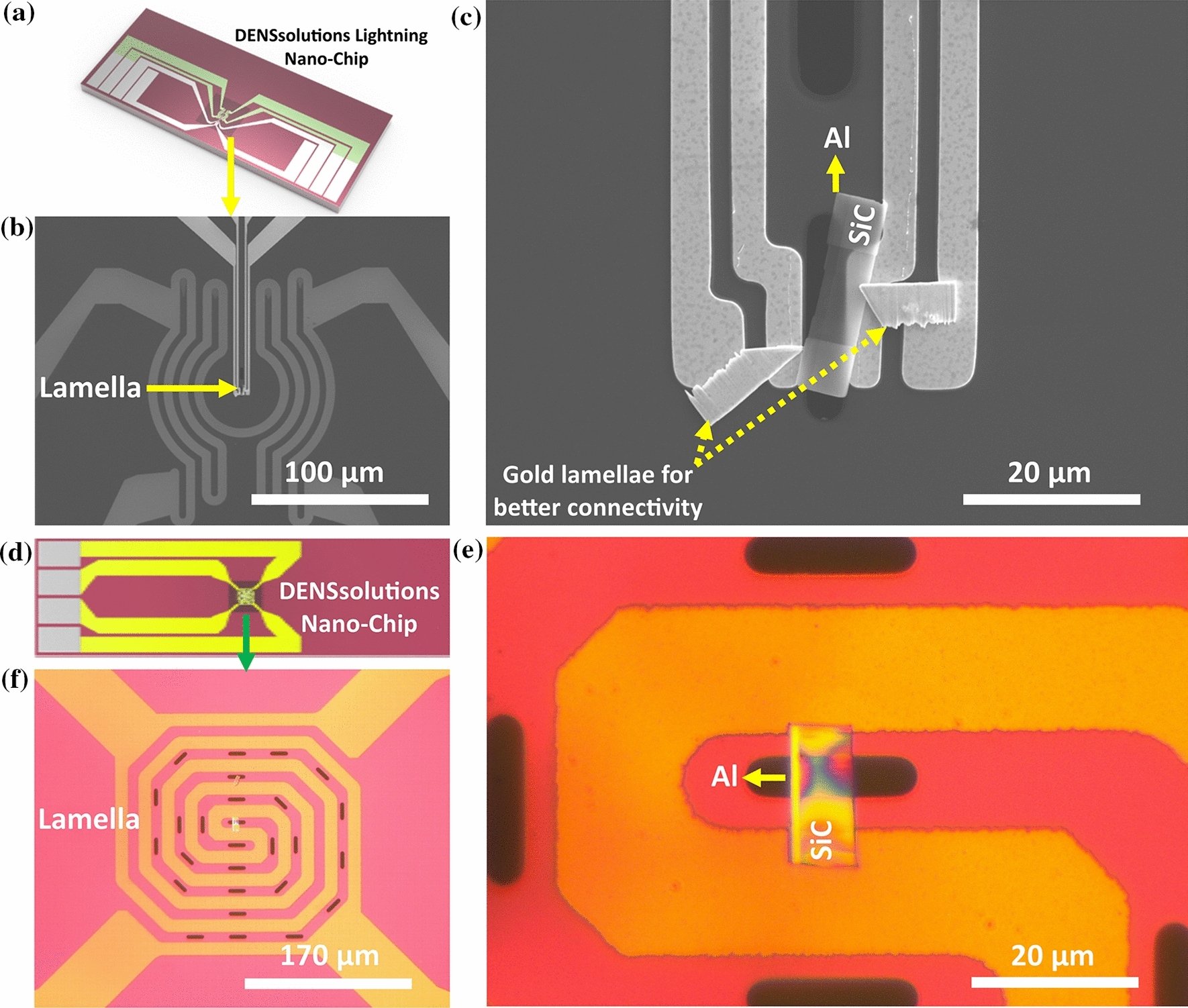
Electron beam-induced current (EBIC) imaging is one of the most powerful techniques for characterizing electrically active defects, junctions, carrier transport and failure mechanisms in semiconductor devices. This work shows how EBIC imaging can be implemented in conventional SEM and STEM instruments, widening access to nanoscale electrical characterization considerably. Samples were biased on DENSsolutions Lightning nano-chips, with the electrical connections in the STEM provided by a Lightning Arctic heating, cooling and biasing holder, and the resulting EBIC images resolve gold nanoparticles at around 1 nm.
Camino, F. et al. Enabling the Acquisition of Electron Beam-Induced Current (EBIC) Images in Conventional SEM and STEM Instruments. Microscopy and Microanalysis 31(5), ozaf080 (2025).