
In Situ TEM

Lightning

In situ TEM heating & biasing

Unprecedented control over the temperature and bias of your sample. Achieve electric fields as high as 300 kV/cm at 900 °C.

Correlate processing, structure, and performance

The Lightning in situ TEM heating and biasing system allows for observing real-time dynamics of your specimen under precisely controlled electrical and thermal environments, while maintaining optimal TEM performance. The holders feature double tilt functionality, enabling atomic resolution imaging and unlocking deeper insights into material properties under simultaneous electrothermal stimuli.

The system expands the analytical capabilities of your TEM, offering a unique platform to link processing conditions with the structure, properties and performance of your materials and devices.

From sample preparation to publishable results

01

Simplified sample preparation

  • High success rate. A verified and reliable lamella preparation process using our dedicated FIB Stub.
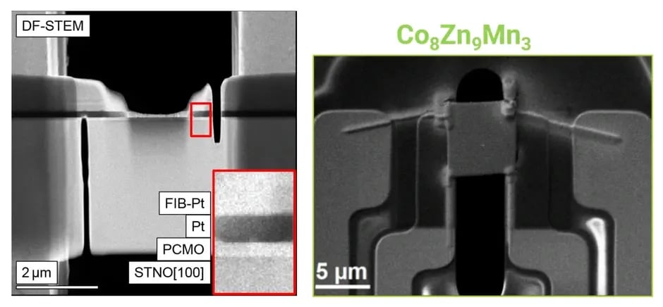
  • Clean FIB lamellae without electrical shorts. Ion milling directly on the SiNx membrane of the chip prepares clean FIB lamellae without compromising heating accuracy and uniformity. It also prevents the electrical short circuits caused by ion redeposition and minimizes leakage currents.

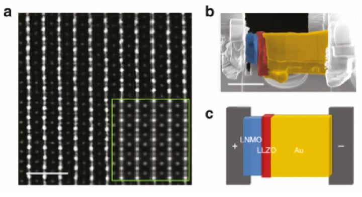
Left: DF-STEM image of a Pt/PCMO/STNO FIB lamella with cuts preventing short circuits across the pn-junction. Meyer et al., J. Phys.: Conf. Ser. 1190 (2019) 012009. Right: SEM image of a Co8Zn9Mn3 TEM lamella on a modified Heating & Biasing chip. Schneider et al., Micros. and Microanal. 30 (2024) ozae044.505.

Read more about the FIB Stub
DF-STEM image of a Pt/PCMO/STNO FIB lamella beside an SEM image of a Co8Zn9Mn3 lamella on a Heating and Biasing chip
02

Reliable stimuli control

  • Heating and biasing accuracy. 4-point probe heating and biasing provides the most accurate temperature, voltage and current control.
  • Broadest electrothermal control. The robust design of the Lightning Nano-Chip withstands up to 150 V (E = 300 kV/cm) in the temperature range from room temperature to 900 °C, while maintaining the best imaging performance.
  • Reliable temperature. Temperature is verified directly in the TEM using EELS and SAED techniques.

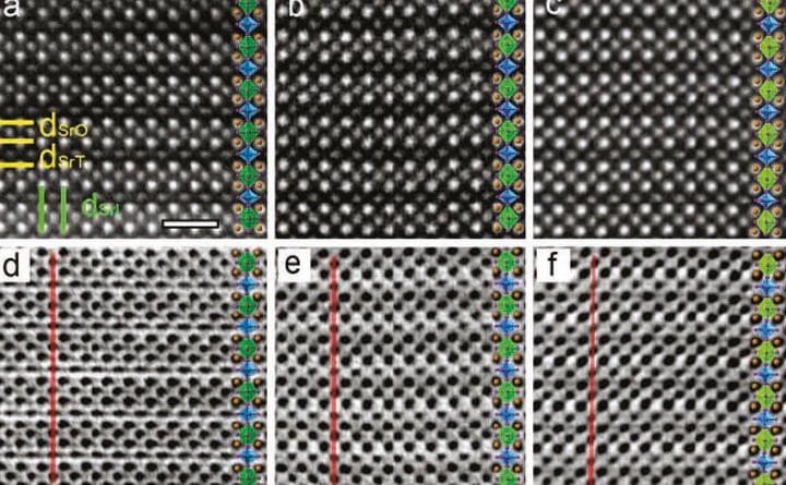
Core-shell nanoparticle at 800 °C while the applied electric field is swept from -21.9 to +21.9 kV/mm, with FFTs of the core and shell (left) and the accompanying vector map (right). Molina-Luna et al., Nature Communications 9 (2018) 4445.

03

High impact results

  • New insights. Perform thermal studies while simultaneously measuring I-V with true pA current sensitivity.
  • High stability while heating and biasing. Minimal sample drift upon heating and biasing enables atomic resolution imaging even at elevated temperatures.
  • Unaffected (S)TEM performance. Minor Z-displacement (bulging) preserves the ultimate resolution without having to perform tedious stage movements.

Sample drift of a Pd nanoparticle over 6 minutes at 800 °C while applying a bias of 40 V. The data has been recorded at the Universidad Complutense de Madrid.

Lightning application fields

Piezo-1

Piezoelectrics

Study ferroelectric domain switching, polarization dynamics and piezoelectric response under applied electric fields at elevated temperatures.

ReRAM

Memory & functional oxides

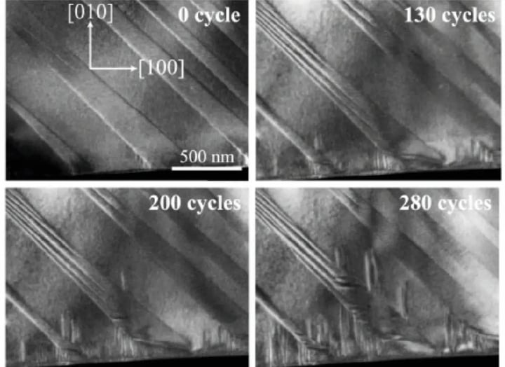
Investigate resistive switching, filament formation and memristive behavior in metal-oxide thin films under electrical stimulus, and follow the oxygen ion migration that drives the structural transformations behind it.

Solar Cells

Solar cells

Observe degradation processes, ion migration and structural changes in perovskite and other solar cell devices under operational bias and temperature.

lightning-piezoelectrics

Solid state batteries

Evaluate battery lifetime and performance by tracking degradation at the solidelectrolyte-electrode interface upon temperature-dependent charge/dischargecycling.

Thermoelectrics res

Thermoelectrics

Observe microstructural changes and identify the precise structural degradation mechanisms and interface changes under continuous thermal and electrical stress.

Simultaneous heating & biasing

The Lightning system combines in situ heating and biasing in a single holder, offering precise control over temperature and electrical bias. It enables electric fields of 300 kV/cm at 900 °C, opening new possibilities for studying electrically active materials. Its stability preserves full atomic resolution and analytical performance during simultaneous heating and biasing experiments.

Nano-Chip

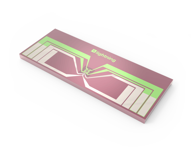
The Lightning Nano-Chips feature a 4-point-probe method to accurately control biasing and heating and retrieve meaningful data. The unique design sustains the highest fields and temperatures to be reached (dedicated or simultaneous) enabling the characterization of today's and tomorrow's advanced materials.
Read more about the Nano-Chip
lightning-nano-chips

Sample holder

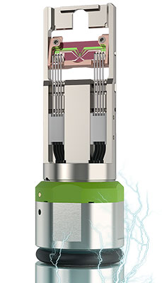
Machined from titanium for ultimate mechanical stability, the Lightning double-tilt holder allocates the Nano-Chip in the microscope. Its versatile design supports all TEM techniques while providing a wide tilt range to examine your sample from optimal angles.
lightning-sample-holder

Hardware & software

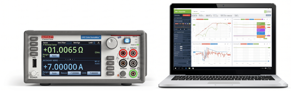
For biasing experiments a source measuring unit (SMU) is required to precisely source voltage or current and simultaneously measure voltage and/or current. The majority of SMUs are compatible with the Lightning system and our preferred supplier/model is Keithley 2450. The Keithley 2450 can conveniently be controlled via our control Impulse software. Different Keithley models or other can be controlled via the manufacturer’s own software. 
Read more about Impulse
Laptop Impulse and Keithley

Nexus

Nexus brings the whole experiment back together in one workspace. Import data from GMS, TIA, Velox, Impulse and more, then visualize your TEM images alongside the electrical and thermal signals on a shared timeline and correct any time offset between datasets. Process the data in the same project with the bundled Python scripts for drift removal, smoothing, peak detection and FFT, or with your own, and the results come back onto the timeline ready to plot and re-run. Annotated videos and figures combining images, graphs and metadata export straight out of it.

Read more about Nexus

What researchers say

Continual advancements of in situ TEM by DENSsolutions provides an exciting and ever-improving level of detail into a range of nano-scale dynamic processes. In particular, the Lightning system allows us to simultaneously heat a FeRh system through magnetic transitions with extreme stability, whilst also applying electrical pulses so that we can drive and visualise magnetic domain wall motion with unparalleled control.
Dr. Trevor Almeida
Dr. Trevor Almeida University of Glasgow
The ability to apply high electric-fields and to simultaneously perform high-resolution experiments at elevated temperatures is frankly impressive! The new and exciting possibilities that the DENSsolutions Lighting series offers trailblazing new directions at the forefront of materials research.
Dr. Leopoldo Molina-Luna
Dr. Leopoldo Molina-Luna Technical University of Darmstadt
In operando TEM observations provide a unique opportunity to visualise the correlations between the electrical properties and the structural changes. The exceptional stability of the DENSsolutions holder allows the in operando TEM experiments to be performed with atomic resolution. Recently, we successfully observed structural changes of resistive switching and organic-inorganic metal-halide perovskite solar cells devices while under electrical stimulus inside a TEM.
Dr. Martial Duchamp
Dr. Martial Duchamp Nanyang Technological University
The DENSsolutions Lightning platform is uniquely suited for high-temperature electrochemical experiments with solid oxide cells (SOCs) due to the exceptionally high electrode-to-electrode inherent resistance of its heating and biasing MEMS chips and the system's low intrinsic capacitance. These specifications are essential for eliminating leakage currents and ensuring reliable electrochemical impedance spectroscopy (EIS) data when characterizing samples in the GOhm range.
Dr. Søren Bredmose Simonsen
Dr. Søren Bredmose Simonsen DTU Energy

Other top research using Lightning

Loading publications…

Frequently asked questions

Find answers to the most common questions about the Lightning.

Is there a procedure that can help me with FIB sample preparation?

Yes, there is a dedicated sample preparation protocol for heating and biasing nano-chips. Furthermore, every Wildfire and Lightning system includes a dedicated FIB stub that facilitates the process (FIB Stub 3.0: Sample Preparation | DENSsolutions).

What is the size of sample recommended for biasing experiments?

The required sample size depends on the specific experiment, the number of electrodes used, and the sample preparation method. Heating and Biasing Nano-Chips feature multiple locations with varying gaps between the electrodes, enabling the placement of samples ranging from 6 μm to 40 μm in length.

Do I need to remove SiN windows for biasing experiments?

When using heating and biasing nano-chips with SiNx windows for biasing experiments, it is advised to remove the corresponding SiNx window to avoid additional electron scattering. SiN windows can be seamlessly removed by the ion beam, which takes roughly a minute or so. It is highly recommended to remove the window prio to FIB lamella transfer to the nano-chip.  

What preparation methods other than FIB could be usable for biasing experiments?

Focused Ion Beam (FIB) is the standard method for preparing lamellae directly onto the Nano-Chip. For alternative workflows, researchers can combine bulk preparation techniques, such as argon (Ar) ion milling or electropolishing with a FIB lift-out process to transfer thin sections. For low-dimensional specimens like nanowires and 2D materials, samples can be transferred to the nano-chip using in situ or ex situ micromanipulators and via standard wet or dry transfer methods, respectively.

What is the maximum temperature?

The maximum temperature for combined electrothermal in situ TEM experiments is 900 °C. For experiments requiring higher temperatures - up to 1300 °C, dedicated heating Nano-Chips need to be used.

Can I perform STEM-EBIC experiments?

Yes, the Lightning system is compatible with the Point Electronic EBIC solution. More information about EBIC experiments using a Lighting system can be found in the following publication:  In‐Operando 4D‐STEM and STEM‐EBIC Imaging of Electric Fields and Charge Carrier Behavior in Biased Silicon p–n Junctions - Moynihan - 2026 - Advanced Electronic Materials - Wiley Online Library.  Please contact us for more information.

Is it possible to apply electrical pulses?

Yes, it is possible to apply electrical pulses. A group from Argonne National Lab were able to successfully apply nanosecond voltage pulses to the sample using DENSsolutions Lightning holder. For more information, please check Nanosecond Structural Dynamics during Electrical Melting of Charge Density Waves in | Phys. Rev. Lett. 

Brochure & application notes

Ready to explore Lightning?

Contact our team to discuss the biasing and heating experiments you have in mind, and receive a tailored Lightning quote.