Semiconductors & Failure Analysis
Watch devices switch, degrade and fail while they operate. At atomic resolution, under live biasing, heating and cooling.
Probe device physics under live operating conditions
Semiconductor devices are becoming increasingly complex as technology nodes continue to shrink and new materials are introduced for advanced logic, memory, power electronics and optoelectronic devices. Understanding electrical behavior, interface evolution, defect formation and failure mechanisms at the nanoscale is therefore essential for improving device performance, reliability and manufacturing yield.
DENSsolutions platforms let researchers combine electrical biasing, heating, cooling and advanced analytical techniques inside the electron microscope, so semiconductor devices can be investigated under realistic operating conditions. From resistive switching and phase-change memory to ferroelectric devices, wide-bandgap semiconductors, EBIC imaging and advanced failure analysis, these capabilities give direct insight into the dynamic behavior of semiconductor devices and functional materials.
Platforms for this research area
Lightning
Precise electrical biasing and Joule heating in the TEM and SEM. Bias a device while you image it to resolve switching, electromigration and interface evolution as they happen.
Lightning Arctic
Cooling, heating and biasing from cryogenic to high temperature. Follow phase transitions and ferroelectric domain dynamics across the full temperature range.
FireBolt
In situ heating and biasing inside the SEM. Localize defects, drive electromigration and study device failure mechanisms on full-size samples without leaving your microscope.
Featured research
Featured experiments
A selection of recent publications enabled by DENSsolutions in situ TEM platforms.
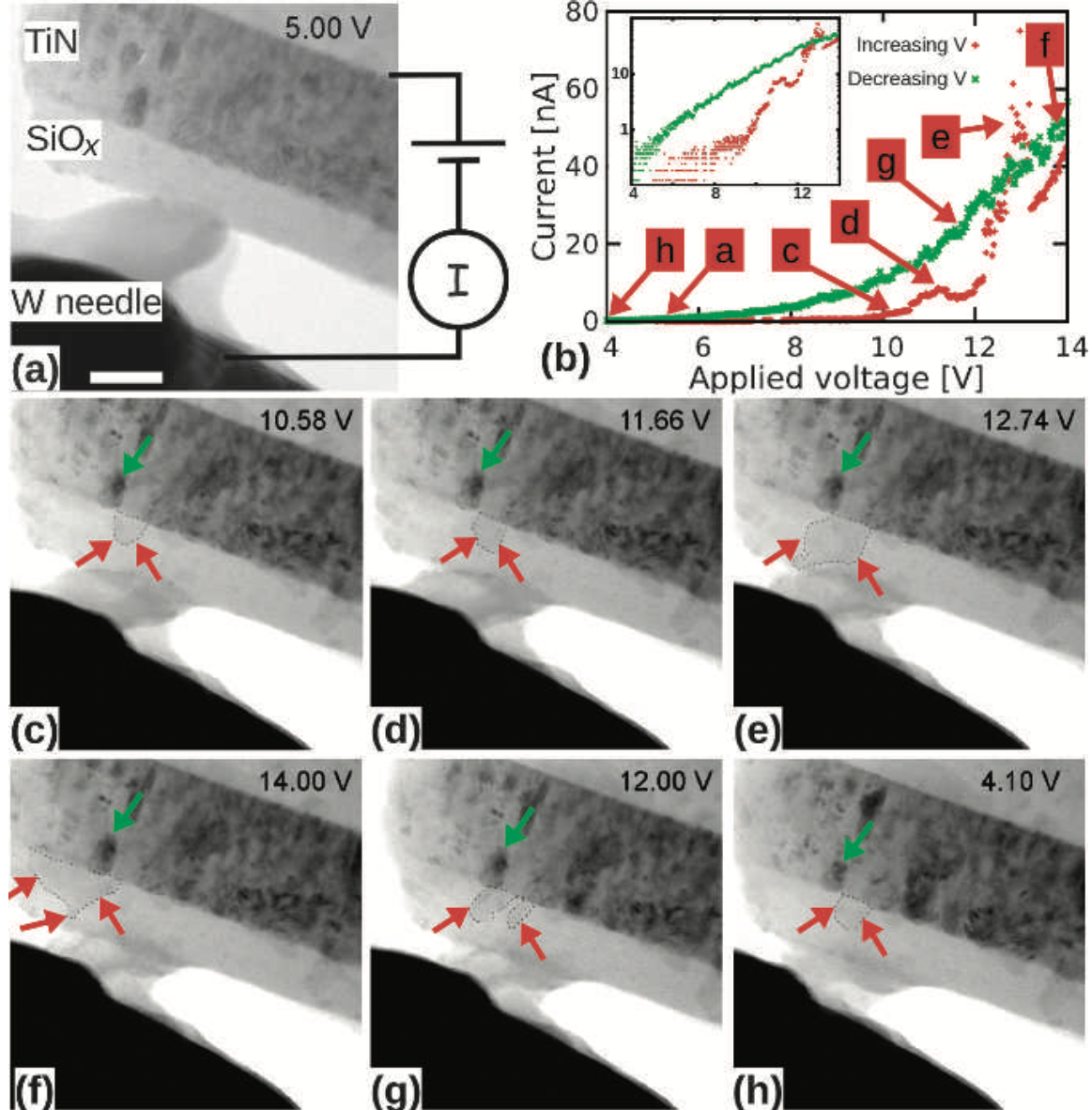
In Situ Transmission Electron Microscopy of Resistive Switching in Thin Silicon Oxide Layers
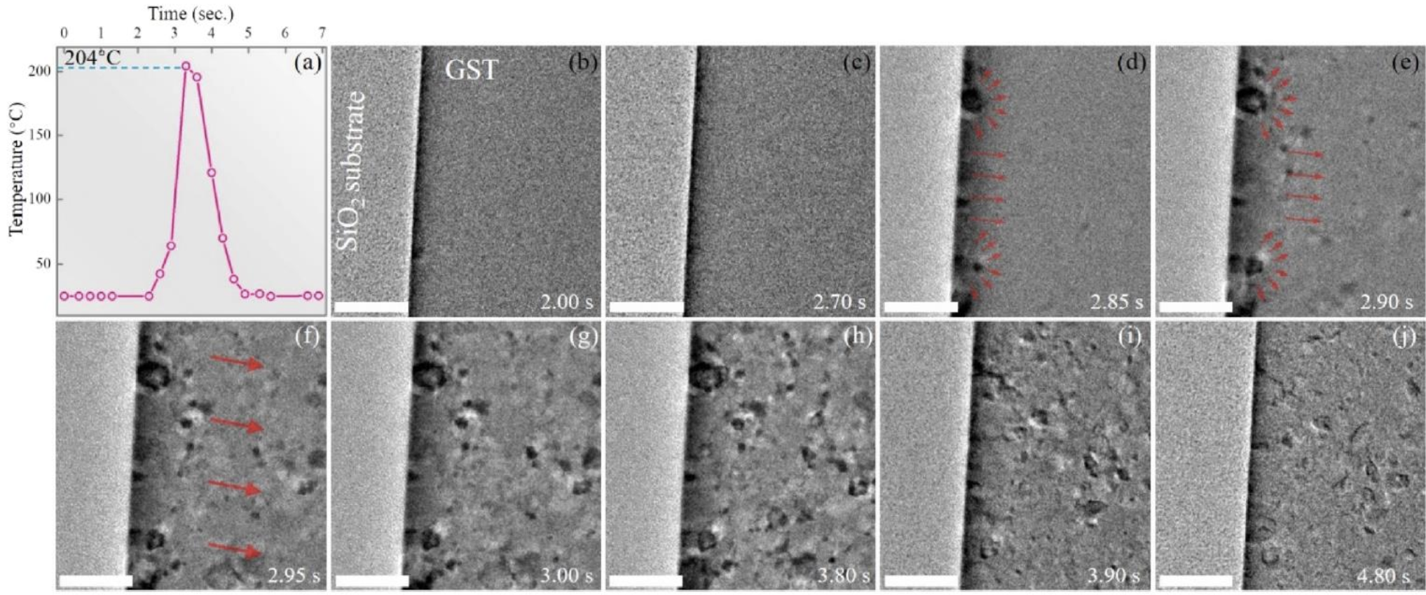
In-Situ Observation of Ge₂Sb₂Te₅ Crystallization at the Passivated Interface
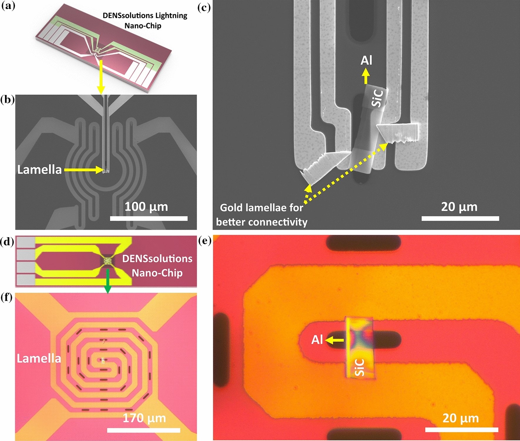
In-Situ Scanning Transmission Electron Microscopy Study of the Al-Amorphous SiO₂ Layer-SiC Interface
Micro-Electromechanical System-Based Cryogenic and Heating In Situ Transmission Electron Microscopy for Investigating Phase Transitions and Domain Evolution in Single-Crystal BaTiO₃
Advance your semiconductor and failure analysis research
Talk to our application specialists to find the right in situ TEM platform for your experiments.
Get in touch