Nano-Chip
MEMS-based heating & biasing
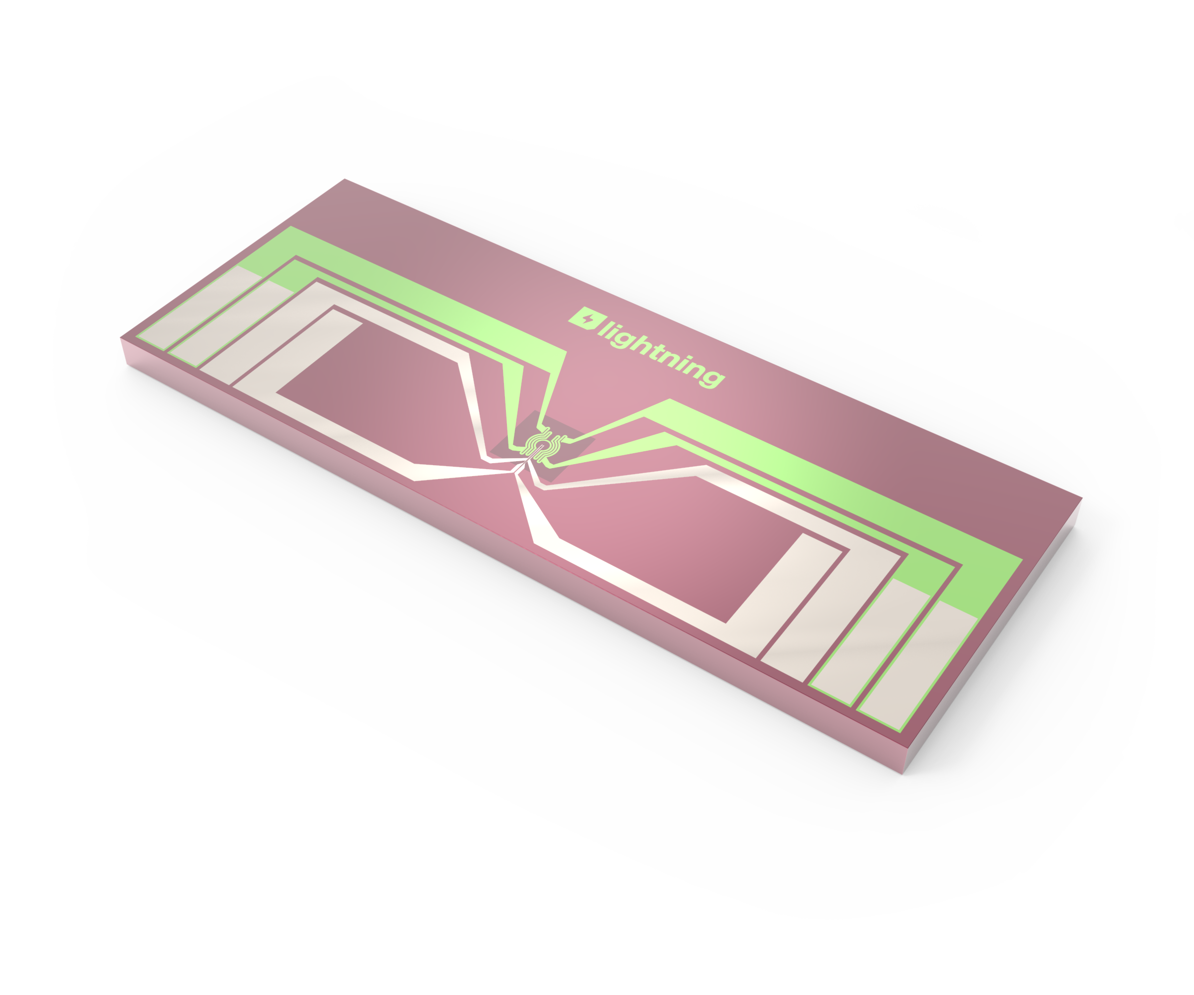
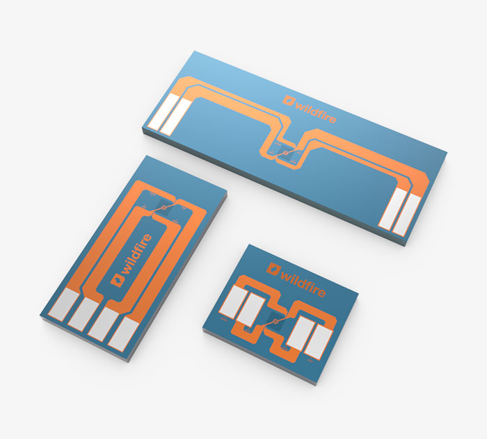
An innovation that enables you to focus on sample and experiment: the Nano-Chip is specifically designed to provide unrivaled sample stability, better homogeneity over the largest viewable area, shortest settling time, higher temperature for EDS and easier sample loading.
MEMS technology
Nano-Chip Specifications
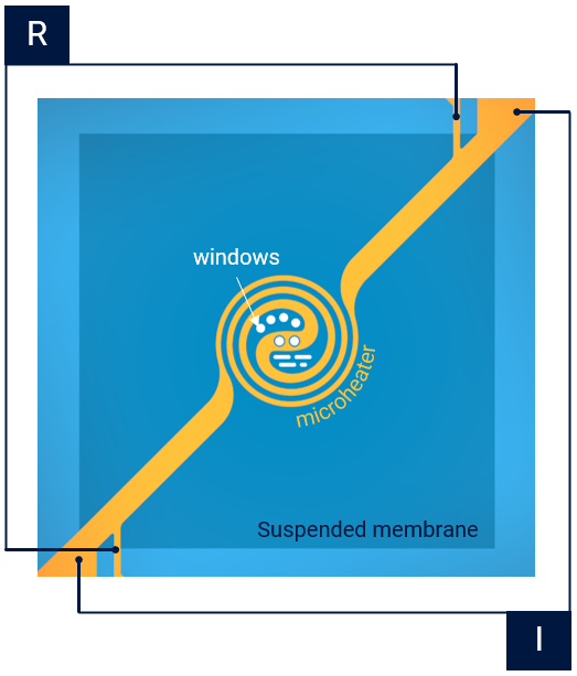
At the core of the Wildfire system is a high-performance MEMS Nano-Chip. By leveraging a refined spiral microheater architecture, the chip achieves exceptional thermal uniformity across the entire viewable area. This design minimizes power consumption and virtually eliminates thermal drift, ensuring your high-resolution imaging remains stable and artifact-free throughout the experiment.
Window designs
Sample preparation made easy
No topography near the windows allows easier thin film (graphene) deposition and eliminates the capillarity effect during drop-casting. Increased membrane stiffness simplifies FIB sample preparation. Multiple windows allow a number of lamellae to be prepared onto the same Nano-Chip.
Viewable area

FIB Lamellas
The circular shape of these windows and the absence of topography around these windows make them ideal for positioning FIB lamellas in any direction.
Best Temperature Homogeneity
These windows are placed in the centre of the microheater and allow the highest temperature homogeneity. Additionally, the surrounding metal further reduces the charging effect.
High Tilting
The elongated windows offer optimal sample visibility at high tilt angles, perfect for tomography.
Nano-Chip performance
Never miss a thing
Directly observe dynamics at the highest resolution after fast temperature change without tedious adjustments. Easily correlate structural transformations with chemical changes of your material at the highest temperature.
Reduced bulging
So far bulging (height change of the membrane while changing temperature and therefore blurred images) was unavoidable. The Nano-Chip’s advanced design minimizes thermal bulging across the entire temperature range, ensuring your sample stays in focus. The Nano-Chip has negligible bulging up to 500 °C.
Sample stability
Apply the largest temperature step and the region of interest (ROI) remains in the field of view with the highest sample stability.
99.5% temperature homogeneity
The Nano-Chip's unique spiral heater design ensures an exceptionally uniform temperature distribution across the entire viewable area. With 99.5% temperature homogeneity, you can be confident that your sample experiences consistent conditions throughout the experiment, eliminating temperature gradients that could compromise your results.

Chemical analysis
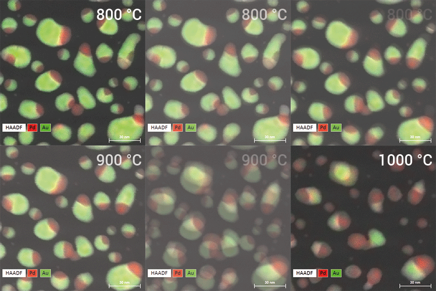
Chemical changes are key to fully understand processes. Due to reduced infrared emission it is now possible to acquire EDS spectra and maps even at 1000 °C.
- 1000 °C: EDS maximum temperature
Guaranteed temperature accuracy
The 4-point-probe measurement enables high temperature accuracy, unrivaled temperature stability and short response time. The accuracy of Wildfire Nano-Chips has been proven by customers using different TEM techniques (EELS and Diffraction).